MoS Rajeev Chandrasekhar to flag off the 2nd SemiconIndia Future DESIGN Roadshow at Bengaluru tomorrow

Union Minister of State for Skill Development & Entrepreneurship and Electronics & IT Rajeev Chandrasekhar will be launching the 2nd Semicon India Future Design Roadshow in Bengaluru on Friday.
The road show is being held with an aim to encourage startups, next-generation innovators, and global & Indian Semiconductor majors to invest in the semiconductor design ecosystem of India.
Rajeev Chandrasekhar has said NextGen devices & electronics products will be architected, designed and co-designed in India, through these schemes like Semicon India Future Design Program.
The 1st event of this series was held at Karnavati University, Gujarat last year.
In December 2021, the Centre had initiated the India Semiconductor Mission with an incentive outlay of Rs 76,000 crore to attract investments in the sector.
“We intend to take the Semicon India program to every student, every college and make as many young Indians excited by and participate in the Semicon India journey,” the Minister said and urged industry leaders, both Global and Indian, to join in making pitch to young students, Startups and entrepreneurs to grab the SemiconIndia FutureDESIGN opportunity.
During the 2nd Roadshow, global semiconductor leaders will be exchanging vision to catalyse semiconductor ecosystem in India.
The announcement of the DIR-V (Digital India RISC-V Microprocessor Program) has set the wheels in motion to develop, Siliconize and create design wins for future around SHAKTI and VEGA RISC-V Processors and India country will witness commercial grade Indian Processors this year. Rajeev Chandrasekhar believes that anyone from anywhere can design Chips and innovate as ChipIN Centre brings semiconductor design facility and Virtual Prototyping Lab to the doorstep.
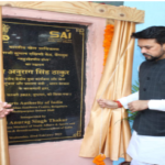
During this roadshow, the Minister will also inaugurate the ChipIN Centre at C-DAC, Bangalore and dedicate its services to semiconductor design community of the country. ChipIN Centre is one of the biggest of existing facilities, offering plethora of design flows, aims to bring the chip design infrastructure at door-steps of entire semiconductor design community in the country. It is a centralized design facility, not only hosting the most advanced tools for entire chip design cycle (i.e. Front-end design, Back-end design, PCB design & analysis etc. for Digital, Analog, RF & Mixed Signal designs), going up to 5nm or advanced node but also provide aggregate services for fabrication of design at SCL foundry & overseas foundries and packaging. It will also enable an arrangement of instructor-led/ online trainings on design flows by industry professionals.
Taking advantage of this, several academic start-ups will mushroom across the country, cross the initial entry barriers and pave the way for entrepreneurship/ startup-led design & innovations ecosystem in the country making indigenous IP Cores, Chips, System on Chip (SoCs), Systems for different application areas like 5G/ IoT, AI/ ML, Automotive & Mobility sector etc. in India, for the World.
During the roadshow, he will also introduce the 1st group of Future Design Start-up which will be supported under the Design Linked Incentive (DLI) Scheme of Semicon India Program. These Start-ups will be working on implementing innovative silicon designs; which will find space in key growth areas- automotive, mobility and computing areas. In coming weeks, more Future Design start-ups are lining up to be approved under the DLI Scheme.


